8255A
Увеличить
Краткое описание:
Programable Peripheral Interface
Дополнительная информация
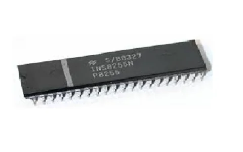
The Intel 8255A is a general purpose programmable I/O device designed for use with Intel microprocessors. It has 24 I/O pins which may be individually programmed in 2 groups of 12 and used in 3 major modes of operation. It interfaces peripheral equipment to the microcomputer system bus.
| PPAP | No |
| I/O Pins | 24 |
| Pin Name | GND0 Volts |
| Cage Code | 4BA62 |
| Automotive | No |
| Package Type | 40 Pin DIP |
| AEC Qualified | No |
| Compatibility | Intel Microprocessor Families |
| RoHS Versions | 2002/95/EC |
| Operating Mode | Mode 2: Bi-Directional Bus (Strobed Bidirectional Bus I/O) |
| Package Type Code | P |
| Power Dissipation | 1Watt |
| Temperature Range | Standard and Extended |
| Radiation Hardening | No |
| Storage Temperature | -65 to +150°C |
| RD=1 to IBF=0 (tRIB) | 300ns |
| System Package Count | Reduced |
| WR=1 to OBF=0 (tWOB) | 650ns |
| ACK Pulse Width (tAK) | 300ns |
| ACK=0 to OBF=1 (tAOB) | 350ns |
| DC Driving Capability | Improved |
| RD=0 to INTR=0 (tRIT) | 400ns |
| STB Pulse Width (tST) | 500ns |
| STB=0 to IBF=1 (tSIB) | 300ns |
| WR=0 to INTR=0 (tWIT) | 850ns |
| ACK=1 to INTR=1 (tAIT) | 350ns |
| I/O Capacitance (CI/O) | 20pF |
| READ Pulse Width (tRR) | 300ns |
| STB=1 to INTR=1 (tSIT) | 300ns |
| WR = 1 to Output (tWB) | 350ns |
| ACK = 0 to Output (tAD) | 300ns |
| Input Capacitance (CIN) | 10pF |
| Input Low Voltage (VIL) | -0.5 to 0.8V |
| WRITE Pulse Width (tWW) | 8255A: 400, 8255A-5: 300ns |
| Input High Voltage (VIH) | 2.0 to VccV |
| Input Load Current (IIL) | ±10µA |
| Data Valid to WRITE (tDW) | 100ns |
| Data Valid from READ (tRD) | 8255A: 250, 8255A-5: 200ns |
| Power Supply Current (Icc) | 120mA |
| Data Float after READ (tDF) | 10 to 150 (8255A), 10 to 100 (8255A-5)ns |
| Output Float Leakage (IOFL) | ±10µA |
| Data Valid after WRITE (tWD) | 30ns |
| Output Buffer Source Current | 1mA at 1.5 volts (for any 8 output buffers from Ports B and C) |
| ACK = 1 to Output Float (tKD) | 20 to 250ns |
| Control Application Interface | Direct Bit Set/Reset Capability |
| Output Low Current (Data Bus) | 2.5mA |
| Ambient Temperature Under Bias | 0 to 70°C |
| Output High Current (Data Bus) | -400µA |
| Peripheral Data after RD (tHR) | 0ns |
| Address Stable after READ (tRA) | 0ns |
| Darlington Drive Current (IDAR) | -1.0 to -4.0mA |
| Peripheral Data before RD (tIR) | 0ns |
| Address Stable after WRITE (tWA) | 20ns |
| Address Stable before READ (tAR) | 0ns |
| Address Stable before WRITE (tAW) | 0ns |
| Per. Data after T.E. of STB (tPH) | 180ns |
| Per. Data before T.E. of STB (tPS) | 0ns |
| Output Low Current (Peripheral Port) | 1.7mA |
| Output High Current (Peripheral Port) | -200µA |
| Time between READs and/or WRITES (tRV) | 850ns |
| Output Low Voltage (Data Bus) (VOL (DB)) | 0.45V |
| Output High Voltage (Data Bus) (VOH (DB)) | 2.4V |
| Voltage on Any Pin with Respect to Ground | -0.5 to +7V |
| Output Low Voltage (Peripheral Port) (VOL (PER)) | 0.45V |
| Output High Voltage (Peripheral Port) (VOH (PER)) | 2.4V |
Если у вас не открывается документ, нажмите, чтобы открыть файл в новой вкладке.


