BSD235CH6327XTSA1
Производится
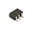
Увеличить
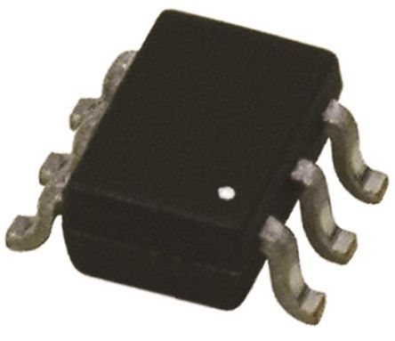
Краткое описание:
N and P-Channel JFET, SOT-363, -20V, 530mA, 500mW
Дополнительная информация
The Infineon BSD235CH6327XTSA1 is a N and P-Channel Junction Field-Effect Transistor (JFET) packaged in a SOT-363 surface mount package. It has a maximum operating temperature range of -55°C to 150°C and a maximum power dissipation of 500mW. The device is halogen free and lead free, and is compliant with RoHS regulations. The JFET has a maximum drain to source voltage of -20V and a continuous drain current of 530mA. The on-state resistance is 350mR, and the input capacitance is 47pF.
| RoHS | Compliant |
| Mount | Surface Mount |
| Series | OptiMOS™ |
| FET Type | N and P-Channel |
| Lead Free | Lead Free |
| Packaging | Cut Tape |
| Rds On Max | 350mR |
| Halogen Free | Halogen Free |
| Package/Case | SOT-363 |
| RoHS Compliant | Yes |
| Package Quantity | 3000 |
| Input Capacitance | 47pF |
| Power Dissipation | 500mW |
| On-State Resistance | 350mR |
| Reach SVHC Compliant | No |
| Max Power Dissipation | 500mW |
| Max Dual Supply Voltage | -20V |
| Max Operating Temperature | 150°C |
| Min Operating Temperature | -55°C |
| Drain to Source Resistance | 266mR |
| Gate to Source Voltage (Vgs) | 12V |
| Continuous Drain Current (ID) | 530mA |
| Drain to Source Voltage (Vdss) | -20V |
Если у вас не открывается документ, нажмите, чтобы открыть файл в новой вкладке.