MM5625
Производится
Увеличить
Краткое описание:
80 Gbps High-Speed Differential Loopback Switch (AC coupled)
Дополнительная информация
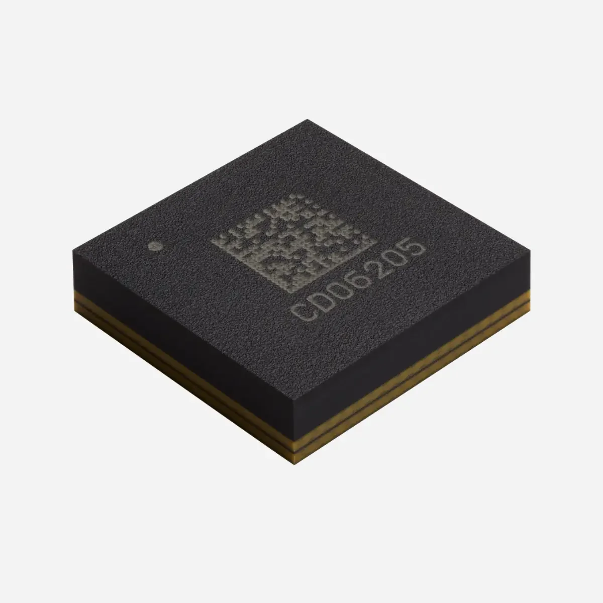
Menlo Micro's MM5625 is an Ideal Switch-based, fully integrated differential DP3T loopback module built for asymmetric SerDes test benches, delivering 80 Gbps (20 GHz) bandwidth so PCIe Gen5/Gen6 and other PAM4 links can be routed, looped back, or isolated without bulky relays. The IMS 2025 launch and the product brief detail its 12-port topology, 128 switch states, on-board charge pump/SPI control, and billions of switching cycles that drastically shorten AI/GPU validation timelines while fitting inside an 8.2 x 8.2 mm LGA SiP.
| Ear | EAR99 |
| RoHS | Compliant |
| Switch Type | Differential Dual DP3T with Loopback |
| Package Type | LGA8.2 x 8.2 mm |
| Actuator Type | Normally Open, Reflective |
| Control States | 128 |
| Datasheet Version | v1.3 |
| SCK Low Time (Min) | 15.5ns |
| Integrated Features | Charge Pump and Driver, AC Coupling Capacitors |
| SCK High Time (Min) | 15.5ns |
| PAM4 Eye Width (0/1) | 10.54ps @ 80 Gbps |
| PAM4 Eye Height (0/1) | 79.74mV @ 80 Gbps |
| SSB Pulse Width (Min) | 15ns |
| Absolute Max Vibration | 500Hz |
| Signal Routing Control | Fully controllable ports |
| PAM4 Total Jitter (0/1) | 7.23ps RMS @ 80 Gbps |
| Start-Up Time (Maximum) | 33ms |
| Start-Up Time (Typical) | 20ms |
| Insertion Loss (Typical) | -2.7dB @ 20 GHz |
| LSB SCK to SSB High (Min) | 15ns |
| Operating Current (IVIND) | 1.7 (typical), 2.75 (max)mA |
| Operating Frequency Range | DC to 20GHz |
| PAM4 Eye Diagram Bit Rate | 80Gbps |
| SPI Clock Frequency (Max) | 33MHz |
| SSB Low to SCK High (Min) | 15ns |
| Switching Cycles (Minimum) | 3 billioncycles |
| Absolute Max RF Input Power | 20dBm into 50 ohms |
| Absolute Max ESD HBM RF Pins | 150V |
| Absolute Max ESD HBM VPP Pin | 500V |
| Absolute Max Mechanical Shock | 500G |
| Power-On-Reset Time (Maximum) | 2.5ms |
| Power-On-Reset Time (Typical) | 1.25ms |
| VIN Current (Dynamic) Maximum | 2.75mA |
| VIN Current (Dynamic) Typical | 1.7mA |
| VIN Quiescent Current Maximum | 2.25mA |
| VIN Quiescent Current Typical | 1.65mA |
| Absolute Max Storage Temperature | -65 to 150°C |
| I/O Logic Supply Current Maximum | 50µA |
| I/O Logic Supply Current Typical | <10µA |
| SDI Valid to SCK Hold Time (Min) | 5ns |
| Absolute Max RF Pin Input Voltage | 3.3V |
| On-State Resistance (RON) Maximum | 4.0Ω |
| On-State Resistance (RON) Typical | 1.7Ω |
| Recommended Operating Temperature | -40 to 85°C Ambient |
| SDI Valid to SCK Setup Time (Min) | 2ns |
| Switch Settling Time (On) Typical | 26.5µs |
| VDD UVLO Rising Threshold Maximum | 2.95V |
| VDD UVLO Rising Threshold Typical | 2.77V |
| Absolute Max Hot Switching Voltage | -0.5 to 0.5V |
| Recommended Switch Cycle Frequency | 100Hz |
| Switch Settling Time (Off) Typical | 9µs |
| VDD UVLO Falling Threshold Maximum | 2.90V |
| VDD UVLO Falling Threshold Typical | 2.72V |
| Low Voltage Digital Current Maximum | 700µA |
| Low Voltage Digital Current Typical | 520µA |
| Off-State Leakage Current (Maximum) | 60nA @ 30VDC |
| Off-State Leakage Current (Typical) | 7nA @ 30VDC |
| Absolute Max Charge Pump Input (VIN) | -0.3 to 5.5V |
| Absolute Max DC Supply Voltage (VDD) | -0.3 to 3.6V |
| Absolute Max Driver Logic Input Levels | -0.3 to VDD_IO + 0.3V |
| Charge Pump Power Supply (VIN) Maximum | 5.5V |
| Charge Pump Power Supply (VIN) Minimum | 4.75V |
| Charge Pump Power Supply (VIN) Typical | 5.0V |
| Logic Reference Level (VDD_IO) Maximum | 5.25V |
| Logic Reference Level (VDD_IO) Minimum | 1.71V |
| Low Voltage Logic Supply (VDD) Maximum | 3.6V |
| Low Voltage Logic Supply (VDD) Minimum | 3.0V |
| Low Voltage Logic Supply (VDD) Typical | 3.3V |
| Absolute Max ESD HBM Control/Power Pins | 2000V |
| Absolute Max I/O Supply Voltage (VDD_IO) | -0.3 to 5.5V |
| SDO Output Valid after SSB Low (Typical) | 20ns |
| SSB Inactive to SDO High Impedance (Max) | 10ns |
| Recommended Charge Pump Power Supply (VIN) | 4.75 to 5.5V |
| Recommended Logic Reference Level (VDD_IO) | 1.71 to 5.25V |
| Differential Isolation (HS1 to HS2) Typical | 46dB @ 20GHz |
| Differential Return Loss (HS1 to HS2) Typical | 18dB @ 20GHz |
| Low Voltage Digital Quiescent Current Maximum | 550µA |
| Low Voltage Digital Quiescent Current Typical | 480µA |
| Recommended Driver Logic Supply Voltage (VDD) | 3.0 to 3.6V |
| Low Voltage Digital Sleep Mode Current Maximum | 10µA |
| Low Voltage Digital Sleep Mode Current Typical | <1µA |
| Differential Insertion Loss (HS1 to HS2) Typical | 2.7dB @ 20GHz |
| Differential Insertion Loss (MS1 to MS2) Typical | 2.2dB @ 16GHz |
| SDO Propagation Delay from SCK Falling Edge (Max) | 10ns |
Если у вас не открывается документ, нажмите, чтобы открыть файл в новой вкладке.