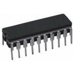
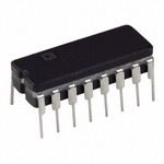
SG1525A
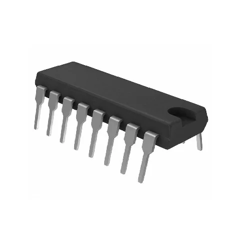
Увеличить
Краткое описание:
REGULATING PULSE WIDTH MODULATOR
Дополнительная информация
The SG1525A/1527A series of pulse width modulator integrated circuits are designed to offer improved performance and lower external parts count when used to implement all types of switching power supplies. The on-chip +5.1 volt reference is trimmed to ±1% initial accuracy and the input common-mode range of the error amplifier includes the reference voltage, eliminating external potentiometers and divider resistors. A Sync input to the oscillator allows multiple units to be slaved together, or a single unit to be synchronized to an external system clock. A single resistor between the CT pin and the Discharge pin provides a wide range of deadtime adjustment. These devices also feature built-in soft-start circuitry with only a timing capacitor required externally. A Shutdown pin controls both the soft-start circuitry and the output stages, providing instantaneous turn-off with soft-start recycle for slow turn-on. These functions are also controlled by an undervoltage lockout which keeps the outputs off and the soft-start capacitor discharged for input voltages less than that required for normal operation. Another unique feature of these PWM circuits is a latch following the comparator. Once a PWM pulse has been terminated for any reason, the outputs will remain off for the duration of the period. The latch is reset with each clock pulse. The output stages are totem-pole designs capable of sourcing or sinking in excess of 200mA. The SG1525A output stage features NOR logic, giving a LOW output for an OFF state. The SG1527A utilizes OR logic which results in a HIGH output level when OFF
| General | LMI level "S" processing available |
| Standard | MIL-M38510/12604BEA (JAN1527AJ) |
| Collector Leakage (VC=35V) | 200µA |
| Logic Inputs (Absolute Max) | -0.3 to 5.5V |
| Analog Inputs (Absolute Max) | -0.3 to VINV |
| Supply Voltage (Absolute Max) | 40V |
| Oscillator Sync Threshold (Typ) | 2.0V |
| Oscillator Clock Amplitude (Typ) | 3.5V |
| Fall Time (Typ, CT=1nF, TJ=25°C) | 50ns |
| Rise Time (Typ, CT=1nF, TJ=25°C) | 100ns |
| Total Standby Current (Typ, VIN=35V) | 14mA |
| Input Voltage (Recommended Operating) | 8 to 35V |
| Reference Load Current (Absolute Max) | 50mA |
| Error Amplifier Output Low Level (Typ) | 0.2V |
| Oscillator Clock Width (Typ, TJ=25°C) | 0.5µs |
| Oscillator Temperature Stability (Typ) | +3% |
| Soft Start Current (Typ, VSHUTDOWN=0V) | 50µA |
| Soft Start Voltage (Typ, VSHUTDOWN=2V) | 0.4V |
| Collector Supply Voltage (Absolute Max) | 40V |
| Error Amplifier Output High Level (Typ) | 5.6V |
| PWM Comparator Input Bias Current (Typ) | 0.05µA |
| Error Amplifier Input Bias Current (Typ) | 1µA |
| Oscillator Current Mirror (Typ, IRT=2mA) | 2.0mA |
| Reference Output Voltage (Typ, TJ=25°C) | 5.10V |
| Storage Temperature Range (Absolute Max) | -65 to 150°C |
| Collector Voltage (Recommended Operating) | 4.5 to 35V |
| Error Amplifier Input Offset Current (Typ) | 1µA |
| Error Amplifier Input Offset Voltage (Typ) | 0.5mV |
| Oscillator Charging Current (Absolute Max) | 5mA |
| Output Drivers Low Level (Typ, ISINK=20mA) | 0.2V |
| Oscillator Initial Accuracy (Typ, TJ=25°C) | 40KHz |
| Output Drivers Low Level (Typ, ISINK=100mA) | 1.0V |
| Reference Output Temperature Stability (Typ) | 20mV |
| Shutdown Delay (Typ, VSD=3V, CI=0, TJ=25°C) | 0.2µs |
| Shutdown Input Current (Typ, VSHUTDOWN=2.5V) | 0.4mA |
| Oscillator Voltage Stability (Typ, VIN=8-35V) | ±0.3% |
| Output Current (Source or Sink, Absolute Max) | 500mA |
| Output Drivers High Level (Typ, ISOURCE=20mA) | 19V |
| Output Drivers High Level (Typ, ISOURCE=100mA) | 18V |
| Reference Load Current (Recommended Operating) | 0 to 20mA |
| Reference Long Term Stability (Typ, TJ=125°C) | 20mV/khr |
| Reference Short Circuit Current (Typ, VREF=0V) | 80mA |
| Undervoltage Lockout (Typ, VCOMP and VSS=High) | 7V |
| Reference Output Noise Voltage (Typ, 10Hz-10KHz) | 40µVrms |
| Reference Output Line Regulation (Typ, VIN=8-35V) | 10mV |
| Reference Output Load Regulation (Typ, IL=0-20mA) | 20mV |
| Oscillator Frequency Range (Recommended Operating) | 100 to 350KHz |
| Deadtime Resistor Range (RD, Recommended Operating) | 0 to 500KΩ |
| Oscillator Maximum Frequency (Typ, RT=2KΩ, CT=1nF) | 350KHz |
| PWM Comparator Maximum Duty Cycle (Typ, VCOMP=3.6V) | 49% |
| PWM Comparator Minimum Duty Cycle (Typ, VCOMP=0.6V) | 0% |
| Thermal Resistance - Junction to Ambient (J Package) | 80°C/W |
| Thermal Resistance - Junction to Ambient (L Package) | 120°C/W |
| Thermal Resistance - Junction to Ambient (N Package) | 65°C/W |
| Operating Ambient Temperature Range (SG1525A/SG1527A) | -55 to 125°C |
| Operating Ambient Temperature Range (SG2525A/SG2527A) | -25 to 85°C |
| Operating Ambient Temperature Range (SG3525A/SG3527A) | 0 to 70°C |
| PWM Comparator Input Threshold (Zero Duty Cycle, Typ) | 0.9V |
| Thermal Resistance - Junction to Ambient (DW Package) | 95°C/W |
| Lead Temperature (Soldering, 10 seconds, Absolute Max) | 300°C |
| Oscillator Sync Input Current (Typ, Sync Voltage=3.5V) | 1.0mA |
| Sink/Source Load Current (Peak, Recommended Operating) | 0 to 400mA |
| Oscillator Minimum Frequency (Typ, RT=150KΩ, CT=0.1µF) | 150Hz |
| PWM Comparator Input Threshold (Maximum Duty Cycle, Typ) | 3.6V |
| Error Amplifier Supply Voltage Rejection (Typ, VIN=8-35V) | 60dB |
| Maximum Shutdown Source Impedance (Recommended Operating) | 5KΩ |
| Error Amplifier DC Open Loop Gain (Typ, RL>=10MΩ, TJ=25°C) | 75dB |
| Oscillator Timing Resistor Range (RT, Recommended Operating) | 2 to 150KΩ |
| Error Amplifier Common Mode Rejection (Typ, VCM=1.5V to 5.2V) | 75dB |
| Oscillator Timing Capacitor Range (CT, Recommended Operating) | 0.001 to 0.1µF |
| Error Amplifier Gain-Bandwidth Product (Typ, AV=0dB, TJ=25°C) | 2MHz |
| Sink/Source Load Current (Steady State, Recommended Operating) | 0 to 100mA |
| Operating Junction Temperature Range (Hermetic/Plastic Packages, Absolute Max) | 150°C |
Если у вас не открывается документ, нажмите, чтобы открыть файл в новой вкладке.