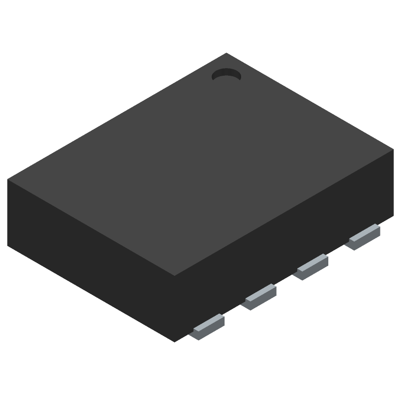
TCK112G,LF
Производится

Краткое описание:
3A Load Switch IC with Slew Rate Control and Reverse Current Blocking
Дополнительная информация
The TCK112G is a high-side load switch IC designed for power management in mobile and portable equipment. It features ultra-low ON resistance of 8.3mΩ and supports a high output current of up to 3.0A. The device operates over a wide input voltage range from 1.1V to 5.5V. Key integrated features include a slew rate control driver to minimize inrush current, a reverse current blocking function, and thermal shutdown protection. Unlike its counterpart TCK111G, the TCK112G includes an automatic output discharge function when the switch is turned off. It is provided in an ultra-small WCSP6C package with a 0.5mm pitch.
| RoHS | Compliant (RoHS3) |
| REACH | Unaffected |
| Switch Type | N-Channel High Side |
| Thermal Shutdown | Built-in |
| Input Voltage Range | 1.1 to 5.5V |
| Output Auto-Discharge | Yes |
| Reverse Current Blocking | Built-in |
| Maximum Output Current (DC) | 3.0A |
| Operating Temperature Range | -40 to 85°C |
| Quiescent Current (ON-state) | 0.02 (typ)µA |
| On-Resistance (RON) @ VIN=1.1V | 8.5 (typ)mΩ |
| On-Resistance (RON) @ VIN=5.0V | 8.3 (typ)mΩ |