UPC451GR-9LG-E1-A
Производится
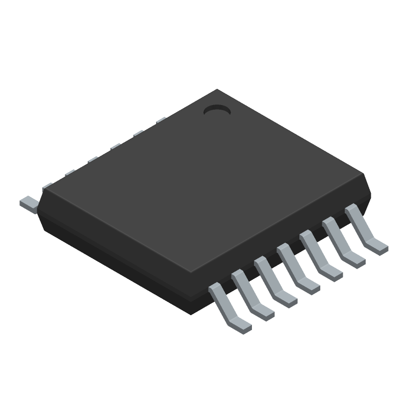
Увеличить
Краткое описание:
Quad Op Amp, 5V, 4 Functions, Voltage-Feedback, 14-Pin, Automotive
Дополнительная информация
Quad operational amplifier featuring a voltage-feedback architecture, designed for single power supply operation. This IC offers four independent amplifier functions within a 14-terminal, 4.4mm x 5.15mm JEDEC R-PDSO-G14 package. Operating across an automotive temperature range of -40°C to 125°C, it supports a nominal supply voltage of 5V with a maximum limit of 30V. Key specifications include a minimum voltage gain of 25,000, a maximum input offset voltage of 7000µV, and a nominal common-mode reject ratio of 85. Frequency compensation is integrated, and the device exhibits micropower characteristics.
| RoHS | Yes |
| REACH | Compliant |
| Width | 4.4 |
| Length | 5.15 |
| HTS Code | 8542.33.00.01 |
| Eccn Code | EAR99 |
| Lead Free | Yes |
| Pin Count | 14 |
| Low-Offset | NO |
| Micropower | YES |
| Architecture | VOLTAGE-FEEDBACK |
| Military Spec | False |
| Amplifier Type | OPERATIONAL AMPLIFIER |
| Voltage Gain-Min | 25000 |
| Temperature Grade | AUTOMOTIVE |
| Terminal Position | DUAL |
| JEDEC Package Code | R-PDSO-G14 |
| Supply Current-Max | 2 |
| Number of Functions | 4 |
| Number of Terminals | 14 |
| Frequency Compensation | YES |
| Input Offset Voltage-Max | 7000 |
| Supply Voltage Limit-Max | 30 |
| Max Operating Temperature | 125 |
| Min Operating Temperature | -40 |
| Supply Voltage-Nom (Vsup) | 5 |
| Bias Current-Max (IIB) @25C | 0.25 |
| Common-mode Reject Ratio-Nom | 85 |
| Neg Supply Voltage Limit-Max | 0 |
| Neg Supply Voltage-Nom (Vsup) | 0 |
| Average Bias Current-Max (IIB) | 0.25 |

