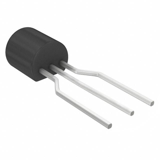
FDG6304P
Производится
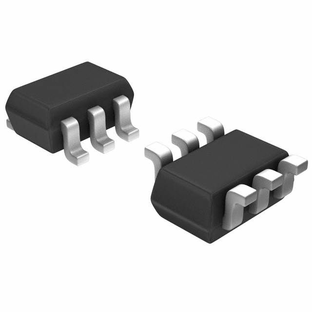
Увеличить
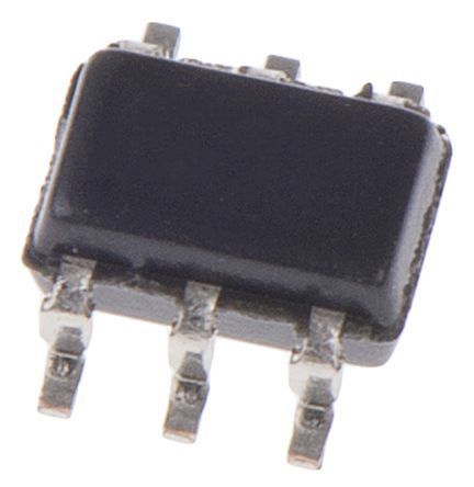
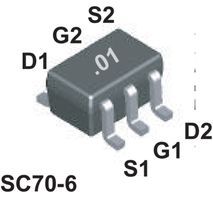
Краткое описание:
Dual P-Channel JFET -25V, 0.41A, 1.1Ω, SC, SMD
Дополнительная информация
Dual P-Channel JFET with -25V Drain to Source Breakdown Voltage and 410mA Continuous Drain Current. Features 1.1 Ohm maximum Drain-source On Resistance and 300mW maximum Power Dissipation. Operates from -55°C to 150°C, with 7ns Turn-On Delay Time and 8ns Fall Time. Packaged in SC for surface mounting, supplied on a 3000-piece tape and reel.
| RoHS | Compliant |
| Mount | Surface Mount |
| Weight | 0.028g |
| Polarity | P-CHANNEL |
| Fall Time | 8ns |
| Lead Free | Lead Free |
| Packaging | Tape and Reel |
| Rds On Max | 1.1R |
| Nominal Vgs | -820mV |
| Termination | SMD/SMT |
| Package/Case | SC |
| Current Rating | -410mA |
| RoHS Compliant | Yes |
| DC Rated Voltage | -25V |
| Package Quantity | 3000 |
| Input Capacitance | 62pF |
| Power Dissipation | 300mW |
| Threshold Voltage | -820mV |
| Number of Elements | 2 |
| Turn-On Delay Time | 7ns |
| Dual Supply Voltage | -25V |
| Radiation Hardening | No |
| Turn-Off Delay Time | 55ns |
| Reach SVHC Compliant | No |
| Element Configuration | Dual |
| Max Power Dissipation | 300mW |
| Max Operating Temperature | 150°C |
| Min Operating Temperature | -55°C |
| Drain to Source Resistance | 1.1R |
| Gate to Source Voltage (Vgs) | -8V |
| Continuous Drain Current (ID) | 410mA |
| Drain to Source Voltage (Vdss) | 25V |
| Drain-source On Resistance-Max | 1.1R |
| Drain to Source Breakdown Voltage | -25V |
Если у вас не открывается документ, нажмите, чтобы открыть файл в новой вкладке.